Selecting ultrasonic cleaning systems semiconductor production can rely on is rarely a simple equipment comparison. In semiconductor cleaning, frequency, chemistry, and tank design work as a single process window, and small mismatches can turn particle removal into surface damage, residue carryover, or unstable yield.
That is why ultrasonic cleaning now receives closer attention across advanced manufacturing support systems. On platforms such as GIAS, this topic sits beside vacuum control, surface treatment, traceability, and other auxiliary technologies that quietly shape product quality, compliance, and long-term process consistency.
Why semiconductor cleaning demands tighter process control
Semiconductor parts are not ordinary machined components. They often include fragile geometries, polished surfaces, narrow channels, bonded features, and high-purity materials that react differently to cavitation energy and wet chemistry.
A cleaning step may target particles, oils, polishing compounds, oxides, flux traces, fingerprints, or packaging debris. Each contaminant behaves differently. Some detach easily. Others smear, dissolve, redeposit, or become more difficult when process parameters are poorly matched.
In this context, ultrasonic cleaning systems semiconductor users evaluate are less about nominal power and more about repeatable control. The goal is not only to make parts look clean, but to reduce hidden contamination that affects downstream coating, inspection, assembly, sealing, or vacuum performance.
What ultrasonic cleaning really does at the part surface
Ultrasonic cleaning uses high-frequency sound waves in liquid to create cavitation bubbles. When those bubbles collapse, they release localized energy that helps dislodge contaminants from part surfaces and hard-to-reach features.
Simple descriptions often stop there, but semiconductor applications need a more practical view. Cavitation intensity changes with frequency, liquid properties, temperature, dissolved gas level, and tank geometry. The same transducer power can behave very differently from one setup to another.
That is also why ultrasonic cleaning systems semiconductor projects should be discussed as part of a broader process-support chain. Cleaning quality affects traceability marking, surface treatment adhesion, vacuum sealing behavior, and even packaging cleanliness.
Choosing frequency by contamination risk and part sensitivity
Frequency selection is usually the first technical checkpoint. Lower frequencies create larger cavitation bubbles and stronger collapse energy. Higher frequencies create smaller bubbles, gentler action, and better penetration into fine structures.
In practice, there is no universal best frequency. The right choice depends on the contaminant load, feature size, substrate fragility, and allowable cleaning time.
Lower frequency may be suitable for robust carriers, metal fixtures, or parts with stubborn machining films. Higher frequency is often preferred for precision ceramic, quartz, wafer handling components, thin metal structures, and surfaces vulnerable to microscopic pitting.
More advanced ultrasonic cleaning systems semiconductor lines use dual-frequency or sweep-frequency operation. These designs help reduce standing wave effects and improve cleaning uniformity across different part shapes.
Questions that clarify frequency selection
- Is the main contaminant particulate, organic, oxide-related, or mixed?
- Are there blind holes, narrow slots, porous surfaces, or fragile edges?
- What level of cosmetic or microscopic surface change is acceptable?
- Does cleaning occur before coating, bonding, vacuum assembly, or final packaging?
Chemistry compatibility matters as much as ultrasonic power
Ultrasonics provide mechanical action, but chemistry often decides whether contamination lifts cleanly or turns into a residue problem. A liquid that dissolves oils well may attack aluminum. A neutral formulation may protect the substrate but leave ionic contamination behind.
For that reason, chemistry selection should be tied to material compatibility, rinse strategy, and disposal requirements, not only to cleaning speed. Semiconductor support environments usually demand lower residue risk, tighter bath control, and more disciplined change intervals.
Common chemistry families include aqueous alkaline cleaners, semi-aqueous blends, neutral precision cleaners, and specialty low-residue formulations. The best option depends on what must be removed and what must remain untouched.
Key chemistry checkpoints
- Compatibility with stainless steel, aluminum, quartz, ceramics, engineered plastics, and elastomers
- Foaming behavior, because excess foam weakens cavitation efficiency
- Rinseability, especially where ionic or film residue can affect downstream cleanliness
- Bath life stability under production load and temperature variation
- Waste handling and regulatory fit for the site or export market
A useful evaluation method is to test the chemistry with representative soils rather than clean sample parts alone. Real contamination often includes mixed oils, particles, polishing compound, and handling residue, and these mixtures expose chemistry limits quickly.
Tank design influences uniformity, not just capacity
Tank design is frequently underestimated. Yet many cleaning failures that appear to be chemistry or frequency issues are actually caused by poor acoustic distribution, weak filtration, or inconsistent part positioning.
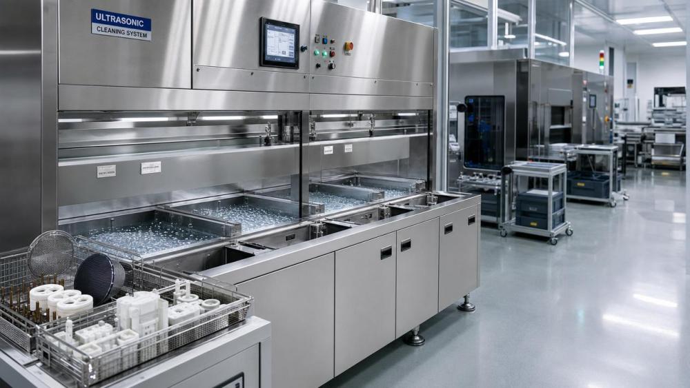
For ultrasonic cleaning systems semiconductor operations require, tank geometry should support stable cavitation across the effective working zone. Dead spots, excessive reflections, and overloaded baskets can create patchy results even when lab trials looked promising.
Tank features worth close review
- Transducer placement and density for even acoustic coverage
- Sweep control to reduce hot spots and standing waves
- Overflow and filtration design to prevent redeposition
- Basket design that avoids shielding and part-to-part contact
- Temperature control with stable heating and sensor accuracy
- Rinse and drying integration where low-residue output is critical
A larger tank is not automatically better. If the working load varies widely, oversized systems may reduce consistency, increase chemistry volume, and complicate control of contamination carryover.
On the other hand, undersized tanks tend to encourage overloading. That usually reduces cavitation access around the parts and makes cycle performance dependent on operator arrangement rather than process design.
Where evaluation often goes wrong
One common mistake is to compare ultrasonic cleaning systems semiconductor buyers shortlist only by frequency and wattage. These numbers matter, but they do not reveal acoustic uniformity, bath contamination control, or actual cleanliness at production scale.
Another mistake is treating cleaning as an isolated station. Semiconductor support processes are linked. If rinsing is weak, drying is inconsistent, or handling after cleaning is uncontrolled, the main ultrasonic stage gets blamed for a broader system issue.
A third problem is using pass-fail visual inspection as the only acceptance method. Precision parts can carry invisible residues that affect adhesion, outgassing, corrosion behavior, or later particle release.
A practical way to compare candidate systems
A structured trial usually delivers more value than a long specification sheet. Start with part families, contamination types, acceptable residue limits, and downstream process sensitivity. Then compare systems under realistic load conditions.
Useful trial inputs include dirty production samples, known defect modes, target cycle time, rinse water quality, drying method, and bath maintenance rules. This approach reflects how advanced manufacturing portals like GIAS frame auxiliary equipment decisions: by connecting machine capability with process outcome.
- Define cleanliness by measurable criteria, not appearance alone.
- Test more than one frequency where the substrate is sensitive.
- Validate chemistry with actual soils and real rinse conditions.
- Check tank loading patterns for shielding and consistency loss.
- Review maintenance needs, bath control, and contamination monitoring.
What to clarify before moving forward
The most reliable ultrasonic cleaning systems semiconductor programs adopt are chosen through process fit, not feature count. Frequency should match part sensitivity. Chemistry should match both soil and substrate. Tank design should support repeatable coverage, rinsing, and contamination control.
The next step is usually to map cleaning requirements against actual failure risks: particle retention, residue carryover, cosmetic change, corrosion, outgassing, or downstream adhesion loss. Once those risks are ranked, equipment comparisons become clearer and far less subjective.
For teams using GIAS as a reference point, that means looking beyond a single machine category and judging how ultrasonic cleaning connects with vacuum integrity, surface readiness, traceability, and overall production consistency. That broader view often leads to better decisions than price or tank size alone.