
How Semiconductor Processing Support Cleanrooms Reduce Contamination Risk in Wafer Handling
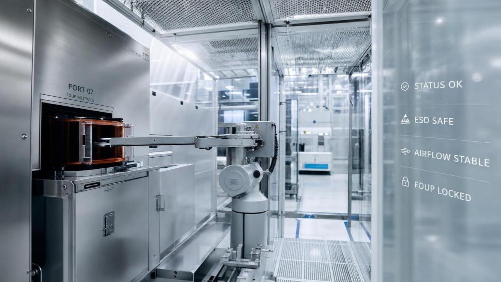
In wafer fabrication, tiny particles can create very expensive failures. A single airborne contaminant may damage patterns, trigger defects, or reduce long-term device reliability.
That is why a semiconductor processing support cleanroom matters far beyond basic housekeeping. It creates a controlled environment around wafer movement, loading, inspection, and temporary staging.
The practical goal is simple. Reduce contamination risk during wafer handling before particles, static, moisture, or unstable airflow can affect process performance.
For operations tied to vacuum systems, cleaning precision, traceability, and process consistency, this support layer becomes a yield protection tool, not just a facility feature.
A well-designed semiconductor processing support cleanroom also helps stabilize interactions between people, tools, carriers, robots, and wafers. That stability is what reduces hidden handling risk over time.
Why wafer handling is especially vulnerable
Wafer handling seems routine, but it exposes sensitive surfaces repeatedly. Transfers between cassettes, FOUPs, aligners, inspection stations, and load ports all introduce contamination opportunities.
Some particles come from operators. Others come from garments, packaging materials, mechanical wear, or poor airflow around automation interfaces.
More subtle risks also matter. Electrostatic discharge can attract particles. Humidity drift can affect static behavior. Temperature variation can change material response or equipment repeatability.
In advanced nodes, the process window is already tight. That means contamination from support activities becomes harder to absorb without yield loss.
- Particle deposition on wafer surfaces or carriers
- Static-driven attraction of airborne contaminants
- Human movement disturbing local laminar airflow
- Mechanical abrasion from transport interfaces
- Humidity and temperature drift affecting stability
A semiconductor processing support cleanroom addresses these risks as a system. It is designed to control contamination pathways before they translate into measurable defects.
How a semiconductor processing support cleanroom lowers contamination risk
The first control point is airborne particle management. High-efficiency filtration, stable pressure differentials, and clean airflow patterns reduce suspended particles near exposed wafers.
The second control point is local handling design. Transfer zones, pass-through interfaces, mini-environments, and tool-loading areas should prevent cross-contamination between adjacent activities.
The third is electrostatic control. Grounding, ionization, conductive materials, and disciplined gowning practices help reduce particle attraction and discharge events.
Environmental stability is another major factor. A semiconductor processing support cleanroom maintains temperature and humidity within narrow ranges so handling conditions stay predictable.
This also improves coordination with vacuum equipment, surface treatment steps, precision cleaning stations, and sensitive inspection systems that depend on repeatable surrounding conditions.
- Filter incoming air to remove fine particles.
- Maintain clean pressure cascades between process areas.
- Control static with ionization and grounded materials.
- Limit operator-generated contamination through procedure design.
- Protect transfer interfaces with enclosed or localized clean zones.
When these measures work together, wafer handling becomes more consistent. That consistency is often the difference between acceptable performance and recurring contamination investigations.
Key design elements to evaluate
Not every clean environment delivers the same result. The design details behind a semiconductor processing support cleanroom determine how well it performs under actual production pressure.
Airflow direction is one of the first points to check. Poorly managed flow can push particles into wafer exposure zones during loading, unloading, or manual intervention.
Materials selection matters too. Interior surfaces, seals, flooring, and transport-contact components should minimize shedding, chemical interaction, and static buildup.
Layout design should separate cleaner and dirtier activities. Maintenance access, packaging movement, and operator routes should not interfere with wafer handling paths.
Monitoring capability is another signal of quality. A semiconductor processing support cleanroom should support particle counts, pressure data, humidity records, and alarm response.
From a technical review standpoint, these factors reveal whether the cleanroom supports stable operations or only meets basic specifications on paper.
Common failure points in support cleanroom performance
Contamination control often weakens at interfaces, not in the main room. Door openings, maintenance panels, material entry points, and robot handoff locations are common examples.
Another issue is treating the semiconductor processing support cleanroom as separate from upstream and downstream equipment behavior. In reality, the whole handling chain matters.
Filters may be well specified, yet airflow balancing may be poor. ESD controls may be installed, yet operator discipline may be weak. Monitoring may exist, yet alarms may lack action rules.
This is why contamination risk should be reviewed as an operating condition, not just a construction feature. Performance under real throughput is what matters.
- Uncontrolled maintenance access near active wafer zones
- Improper gowning and material transfer procedures
- Particle-generating contact surfaces in transport hardware
- Weak integration between cleanroom alarms and response actions
- Humidity drift increasing electrostatic sensitivity
A capable semiconductor processing support cleanroom should reduce these weak points through design, operating discipline, and verifiable maintenance routines.
What to ask when comparing solutions
When reviewing suppliers or internal proposals, the right questions are often more useful than broad specification sheets. They expose whether contamination control is truly engineered.
Start with application fit. A semiconductor processing support cleanroom for wafer handling should match wafer type, automation level, process sensitivity, and maintenance frequency.
Then examine how the environment supports adjacent auxiliary systems. Vacuum stability, precision cleaning, surface condition control, and traceability processes often intersect in the same workflow.
More importantly, request proof of repeatability. Data from particle mapping, airflow visualization, ESD validation, and operational qualification tells a clearer story than marketing language.
- How is airflow protected at wafer handoff points?
- What controls are used for static-sensitive operations?
- How are material entry and maintenance access separated?
- What monitoring data is continuously recorded?
- How is cleanroom performance verified after changes or repairs?
- Which contamination events have been reduced in similar installations?
These questions keep the discussion practical. They help link a semiconductor processing support cleanroom directly to yield, uptime, and long-term process consistency.
A practical path to better wafer handling control
The strongest contamination strategy usually starts with mapping the full wafer journey. Identify where exposure occurs, where particles may be introduced, and where static conditions can change.
Next, align the semiconductor processing support cleanroom with those specific risks. That may involve airflow redesign, local enclosures, ESD upgrades, cleaner materials, or tighter transfer discipline.
After implementation, confirm performance with data. Measure particle behavior at critical handling points, review alarm trends, and compare defect rates before and after changes.
This approach turns the semiconductor processing support cleanroom into an active contamination-control solution. It supports wafer quality, protects equipment reliability, and strengthens manufacturing consistency over time.
In practical terms, cleaner handling conditions reduce avoidable risk. And in semiconductor production, reducing avoidable risk is often where the most durable process gains begin.