
Why Precision Wafer Surface Coating Matters More Than Ever
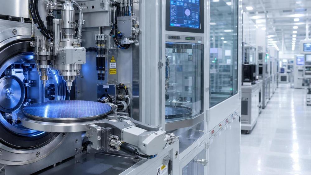
In semiconductor production, small coating errors rarely stay small for long.
A slight thickness shift can weaken adhesion, distort pattern transfer, or trigger yield loss downstream.
That is why precision wafer surface coating is not just a materials issue.
It is a process control issue tied directly to repeatability, contamination risk, and equipment capability.
As device structures shrink and layer stacks become more complex, coating windows get tighter.
The same applies in MEMS, compound semiconductors, advanced packaging, and precision optics.
In practical terms, precision wafer surface coating affects three outcomes that every factory tracks closely.
- Adhesion between the wafer and the deposited or applied layer
- Uniformity across the full wafer surface and from wafer to wafer
- Yield stability through lithography, etch, deposition, bonding, and final inspection
This also explains why buyers now look beyond headline throughput.
They want evidence that coating tools can hold process consistency under real production conditions.
How Precision Wafer Surface Coating Improves Adhesion
Adhesion starts at the interface, and the interface is unforgiving.
If the wafer surface carries residual particles, organic films, moisture, or uneven surface energy, coatings attach inconsistently.
Precision wafer surface coating helps by controlling both preparation and application.
On the preparation side, surface activation and cleaning are critical.
Plasma treatment, wet cleaning, dehydration bake, and adhesion promoters all influence bond quality.
On the application side, fluid delivery, dispense volume, spin profile, and ambient conditions matter just as much.
A well-tuned precision wafer surface coating process reduces local weak points.
That lowers the chance of peeling, blistering, edge lift, and delamination during later thermal or chemical exposure.
More importantly, strong adhesion is not only about passing one test coupon.
It must remain stable through storage, handling, patterning, curing, and assembly.
Key adhesion variables to evaluate
- Surface cleanliness before coating
- Surface energy consistency across the wafer
- Primer or adhesion promoter compatibility
- Coating viscosity control and solvent balance
- Temperature and humidity stability during application
- Post-coat bake and cure profile repeatability
From a technical review standpoint, adhesion data should always be linked to process conditions.
A strong result without context is difficult to trust at production scale.
Uniformity Is the Real Test of Process Maturity
Many coating systems can create a good-looking wafer once.
The harder question is whether they can do it repeatedly across many lots.
That is where precision wafer surface coating becomes a serious benchmark.
Uniformity affects line width control, etch behavior, dielectric performance, stress distribution, and optical response.
Even a small center-to-edge variation can amplify during later process steps.
For photoresists, that can change exposure latitude and critical dimensions.
For barrier or protective films, it can create weak areas and inconsistent protection.
What drives uniformity in precision wafer surface coating
Uniformity depends on more than spin speed alone.
- Dispense nozzle accuracy and droplet behavior
- Wafer centering and chuck stability
- Fluid temperature and viscosity drift
- Airflow design inside the coating chamber
- Edge bead control and solvent evaporation rate
- Recipe repeatability across product changes
A mature precision wafer surface coating system also needs strong metrology feedback.
Thickness maps, defect inspection, and SPC trends reveal whether apparent stability is actually real.
This matters even more when fabs run multiple materials or frequent recipe changes.
The Yield Connection: Where Coating Precision Pays Off
Yield loss often appears later than the coating step that caused it.
That delay makes root-cause analysis harder and equipment comparison more important.
Precision wafer surface coating improves yield by reducing hidden variability at the start.
When adhesion is stable and film thickness is consistent, downstream steps behave more predictably.
This means fewer reworks, fewer scrap wafers, and tighter process windows.
In high-value production, that financial impact is substantial.
Common yield risks tied to weak coating control
- Pattern collapse or incomplete transfer
- Microvoids, pinholes, or local thin spots
- Cracking after bake, cure, or thermal cycling
- Particle entrapment that seeds defect clusters
- Bonding failure in advanced packaging flows
- Electrical leakage caused by incomplete coverage
A useful evaluation method is to connect coating performance with actual line yield indicators.
That includes defect density, rework rate, lot deviation, and excursion frequency.
This approach gives a clearer picture than standalone lab data.
What to Check When Comparing Coating Equipment and Processes
Not every vendor defines precision the same way.
Some focus on nominal thickness results under ideal conditions.
Others can document long-run stability, contamination control, and maintenance behavior.
For precision wafer surface coating, the second group usually provides more reliable decision value.
A practical technical evaluation checklist
- Review thickness uniformity data by wafer size, material type, and production duration.
- Check contamination management, including chamber cleanliness and chemical handling design.
- Ask how the system controls humidity, temperature, and solvent evaporation.
- Verify recipe repeatability after tool cleaning, maintenance, or material changeover.
- Request adhesion and defect data under thermal stress, not only at room conditions.
- Confirm metrology integration, SPC support, and alarm traceability.
- Look at consumables stability, waste management, and uptime impact.
It is also worth checking whether the process supports future materials.
That includes low-k films, specialty resists, wafer-level packaging layers, and advanced protective coatings.
A tool that performs well today but lacks process flexibility can become a bottleneck quickly.
Standards, Process Discipline, and Long-Term Reliability
Precision wafer surface coating should be reviewed against both technical data and process discipline.
That means documented procedures, traceable parameters, and consistent inspection methods.
In regulated or export-facing manufacturing, documentation quality matters almost as much as film quality.
Reliable records support qualification, audits, customer approval, and process transfer between sites.
This is where broader auxiliary systems also come into play.
Cleaning precision, vacuum stability, traceability marking, and batch control all shape coating outcomes.
Seen this way, precision wafer surface coating is part of a larger manufacturing control architecture.
The most dependable lines treat it as an integrated quality function, not a standalone station.
The bottom line is straightforward.
Precision wafer surface coating improves adhesion by stabilizing the interface.
It improves uniformity by controlling material flow, environment, and repeatability.
And it improves yield by removing variation before it multiplies across the line.
For any technical assessment, the most useful question is not whether a coating tool can run.
It is whether its precision wafer surface coating performance stays stable under real manufacturing pressure.
That is usually where long-term value becomes visible.